Prashant Mangal
Analog IC Designer
WIDE RANGE DELAY LOCKED LOOP
In a memory interface Double Data Rate (DDR) standard is commonly used to achieve higher baud rate. Typically a memory controller sends bursts of data with a synchronized clock to the receiving slave unit. The receiver samples the data on both the rising and falling edges with respect to the received clock. Thus this is referred to as Double Data Rate or DDR.
During a typical DDR Interface, the received clock and data are not aligned perfectly. A Delay Locked Loop (DLL) is used to shift the data with respect to the clock so that the sampling is done at the center of the eye. DDR standards range from several hundreds of MHz all the way up to GHz. This necessitates a DLL design that accommodates the broad frequency range.
Previous and current DLL designs do not have wide frequency range of operation. Their range is limited to a couple of hundred MHz which is centered at a specific frequency. This severely limits the operation to a specific standard frequency and cannot be used across all DDR standards.
This design provides a wide range DLL which can range from 200MHz to 1.6GHz. The frequency (delay) lock range extends beyond 1GHz and can support all DDR standards. This is achieved by having a Voltage Controlled Delay Line (VCDL) with variable frequency bands. The locking mechanism locks on to the incoming reference clock by jumping though the bands in a deterministic manner avoiding any false locks. The system responds to an incoming clock fast and a clean lock is acquired within 1024 reference clock cycles.
Description
Figure 1 shows the embodiment of the design. The Wide Range DLL consists of a typical DLL loop with Multi Band Voltage Controlled Delay Line (VCDL) with a Digital Controller and a Lock Detect circuit.
The Phase Frequency Detector (PFD) compares the Input Reference Clock to the Feedback Clock from the VCDL and generates UP/DOWN signals. These Up/Down signals from the PFD are fed to the Charge Pump which integrates these pulses to generate a Control Voltage (Vcontrol). The Control Voltage modulates the delay of the VCDL.
The Digital Controller selects the appropriate frequency band for the Multi Band VCDL. This selection is governed by the Control Voltage level which is detected by a Comparator comparing VC to a Reference Voltage (Vref).
The Lock Detect circuit detects if the VCDL is in slow or fast or in lock condition by analyzing 8 phases. It also has a Charge Pump Control (Release) which overrides the main loop until the correct frequency band is determined for the VCDL. This avoids any false lock condition.

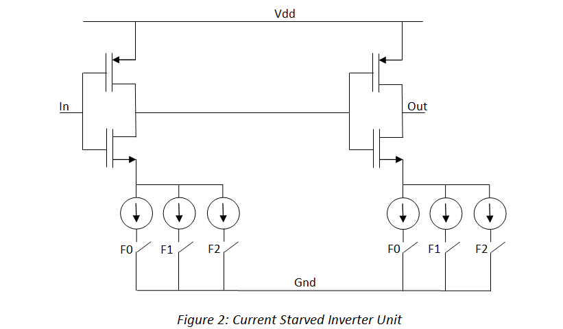
Figure 2 shows the details of a single unit of the Multi band VCDL. It consists of a Current Starved Inverter with 3 selections for current. This allows 8 different strengths of current for a single unit. Each selection translates to a specific frequency band of VCDL operation.
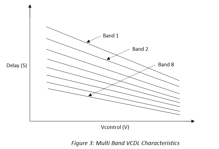
Figure 3 shows the Multi Band VCDL versus Control Voltage graph.
Operation
The locking mechanism of this DLL starts when a Reference Clock is applied. The Digital Controller asserts a RESET to clear the states of all circuits and pre charge the Control Voltage to the highest voltage. It then selects the maximum current strength for the VCDL which puts it in the fastest frequency band. The Lock Detect circuit overrides the main DLL loop by ramping down the Control Voltage in a controlled manner. While this is happening, the Lock Detect circuit is also determining if the VCDL is slower or faster than the REF.
The Digital Controller starts off by selecting the fastest frequency band for the VCDL and works its way down to the slower frequency bands algorithmically as determined by the Control Voltage level and the DLL Lock signal. Once the DLL has acquired lock and the VC level is above the Reference Voltage a steady state is achieved.
This is depicted in Figure 4.
Variations
The Wide Range DLL shown here operates from 200MHz to 1.6GHz. This uses 3 current selections in the Current Starved Inverter to generate 8 different VCDL frequency bands. By adding more current selections to the Current Starved Inverter more frequency bands can be generated to achieve even wider locking range.
This provides great flexibility to target different data rates and ranges.

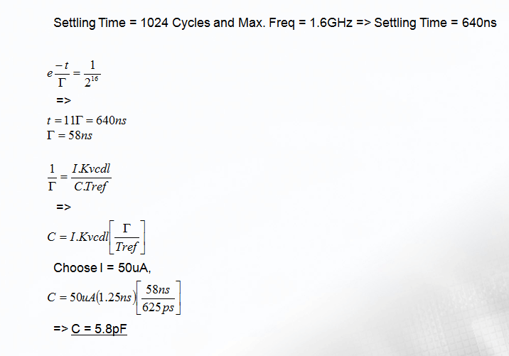
DLL Equations